
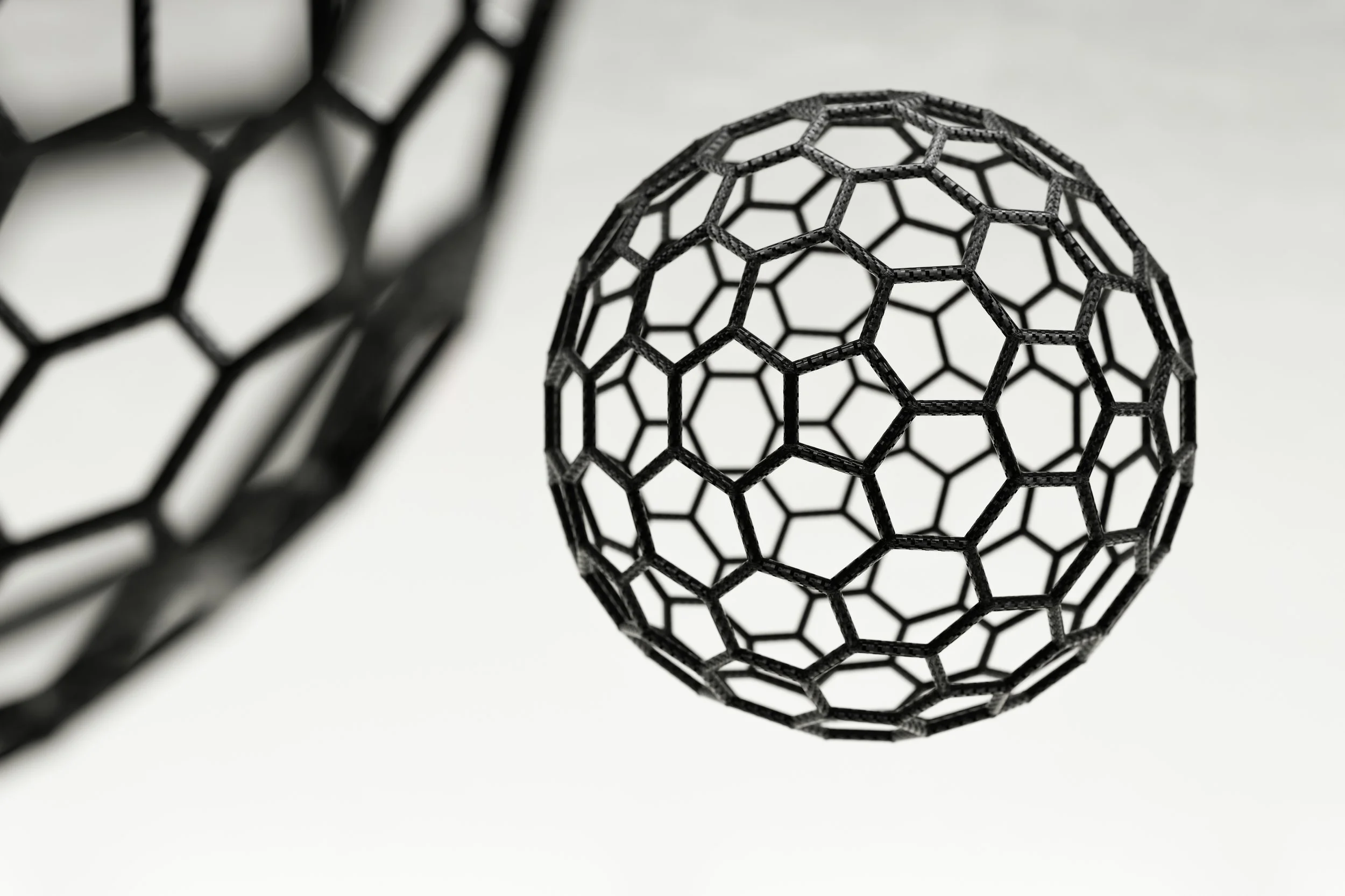
Interlayer Materials

Electron and hole transport layers are among the most performance-critical components in a photovoltaic device stack. Nano-C's interlayer materials have been used in some of the highest-performing and most stable perovskite and thin-film PV devices produced to date.
Nano-C's portfolio spans fullerene ETLs and organic molecule-based HTL materials, with an expanding lineup in active development. Whether you're optimizing an existing stack or developing a new architecture, Nano-C works directly with research and production teams to find the right solution.

Nano-C: Engineered at the Interface.
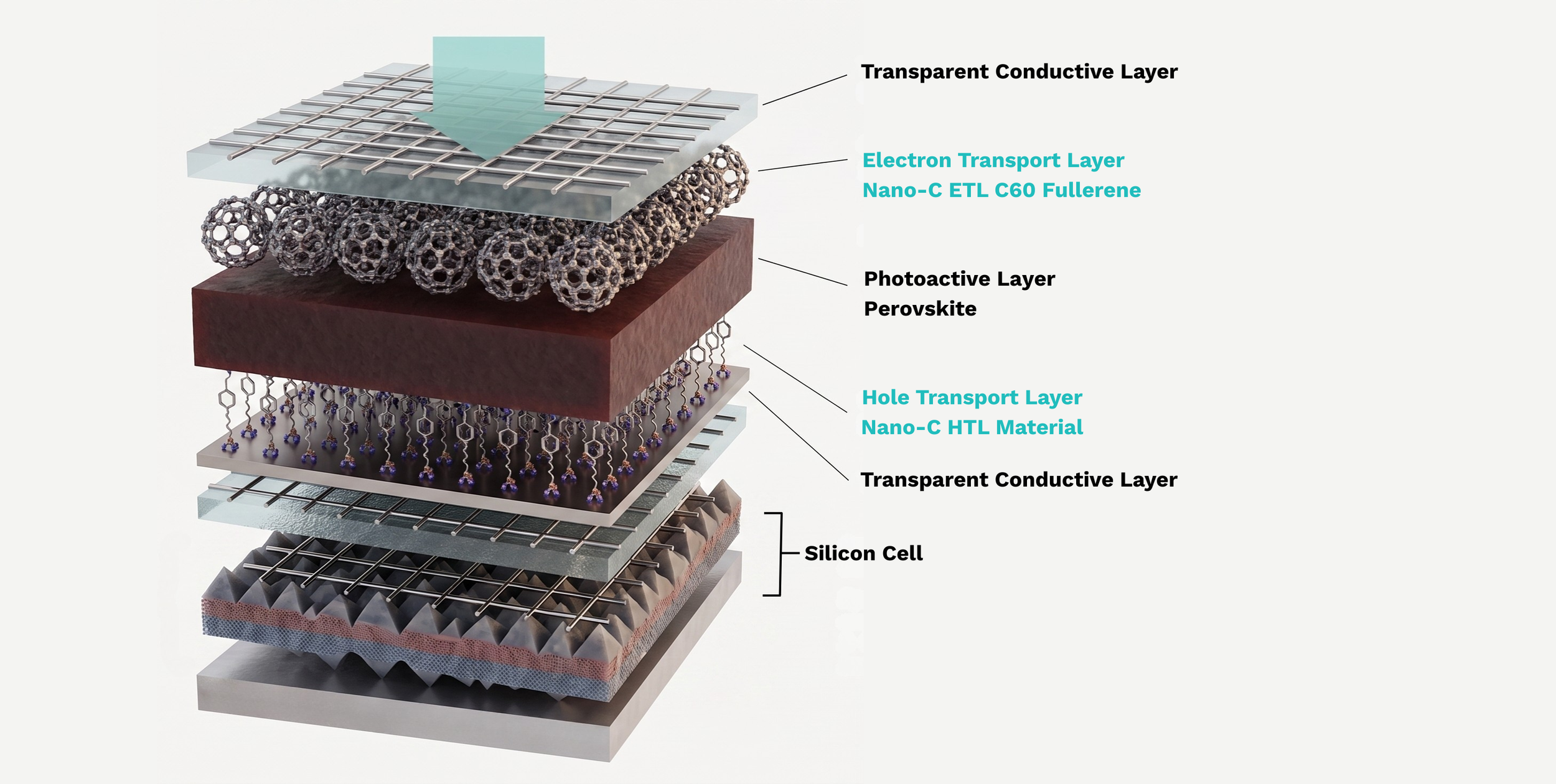
Tandem Perovskite Solar p-i-n Device Structure
Electron Transport Layers
An effective ETL aligns the conduction band or LUMO level between the absorbing layer and the cathode level, enabling efficient electron extraction while blocking holes. Misalignment at this interface drives recombination and erodes performance.
Nano-C's ETL portfolio is engineered to minimize these losses. Our materials are optimized for precise energy level tuning across a range of device architectures, with particular attention to interface chemistry and compatibility with perovskite absorber compositions.
Key performance considerations our ETLs address:
Energy level alignment for low-loss electron extraction • Reduced interfacial trap density and recombination • Chemical compatibility with mixed-halide and Cs/FA perovskite blends • Hysteresis mitigation through improved ETL/perovskite interface quality
Hole Transport Layers
The HTL mirrors this function on the anode side, bridging the HOMO level of the absorbing material and the work function of the conducting electrode to enable efficient hole extraction.
For perovskite solar cells, particularly p-i-n structures used in tandem PV, the HTL must also serve as a high-quality substrate for perovskite crystal growth. Crystallinity at this interface directly impacts both efficiency and operational lifetime. Nano-C's HTL portfolio includes 0PATPA, a SAM-based material engineered specifically for this interface challenge.
Key performance considerations our HTLs address:
Precise energy level alignment for efficient hole extraction • SAM-enabled interface tuning for enhanced electrical performance • Improved perovskite crystal quality and morphology • Active layer protection during subsequent deposition steps • Stability under thermal and operational stress conditions

Self-Assembled Monolayer (SAM) Materials
SAMs represent a new generation of interface engineering. By forming ordered molecular layers at the HTL surface, SAMs enable precise control of surface energy and electronic properties that conventional HTLs can't match, with the added advantage of low-temperature, solution-based deposition compatible with scalable manufacturing. Nano-C's growing SAM portfolio is available for collaborative development and stack optimization. Contact our technical team to learn more.

Your Stack. Our Expertise.
Device stacks are not generic, and the optimal interlayer solution depends on your specific absorber composition, architecture, and processing constraints. Nano-C offers materials selection, formulation development, and stack optimization support, working directly with your team to identify and refine the right ETL or HTL for your application.